|
Financial source: Junta de Andalucía / Fondos FEDER Code: FEDER-US-1263142 Acronym: PlasmaCells |
Tecnología de plasma para el desarrollo de una nueva generación de conductores de huecos en celdas solares de perovskita.Principal Investigator: Period: Research team: José Cotrino, Angel Barranco , Juan Pedro Espinós, T. Cristina Rojas. |

Las celdas solares (CSs) de tercera generación son dispositivos nanotecnológicos que convierten directamente la luz solar en electricidad y suponen el paradigma de la investigación en energías renovables de cuyo aprovechamiento dependerá el futuro energético del planeta. Recientemente, un ejemplo particular de CSs que contienen una perovskita de haluro organometálico como absorbedor de luz han centrado la atención de la comunidad científica debido, ante todo, a su alta eficiencia y bajo coste. Estas características las convierten en una alternativa prometedora a las celdas actuales (de Si y calcogenuros). Sin embargo, para que la realización final y comercial de las celdas de perovskita sea posible es necesario que alcancen una mayor estabilidad, durabilidad y reproducibilidad. Los avances más importantes alcanzados se han debido a la intensa investigación sobre los elementos que integran esta CS: conductor de electrones, perovskita y conductor de huecos. En concreto, este último elemento ha tenido una importancia crucial en su evolución tras la implementación de los conductores de huecos en estado sólido.
PlasmaCells persigue abordar por primera vez la síntesis de una nueva familia de conductores de huecos por técnicas de vacío y plasma. Estas metodologías son escalables industrialmente y presentan grandes ventajas con respecto a las metodologías en disolución (las más usadas), entre las que destacan: su alta versatilidad, control de composición y microestructura, bajo coste, que son respetuosas con el medio ambiente ya que no precisan disolventes, no producen emisiones contaminantes y son compatibles con la tecnología actual de semiconductores.
El objetivo principal de PlasmaCells es la integración de estos nuevos conductores de huecos procesados por plasma en CSs de perovskita. La importancia del proyecto se basa en resultados recientes obtenidos por el Investigador Principal (IP) que demuestran que la aproximación propuesta puede ser una de las vías más prometedoras para el aumento de la estabilidad, durabilidad y reproducibilidad de estas CSs, que actualmente suponen el cuello de botella que impide su industrialización. Cabe destacar que no existe en la bibliografía ningún ejemplo sobre esta aproximación sintética para el desarrollo de conductores de huecos. Se espera que esta oportunidad permita demostrar las ventajas y versatilidad de esta metodología innovadora en un campo de alto impacto, que se enmarca dentro de las áreas prioritarias RIS3 Andalucía y en el PAIDI 2020 de crecimiento sostenible, eficiencia energética y energías renovables.
|
Financial source: Agencia Andaluza del Conocimiento Andalucía Talent-Hub |
Purely organic and hybrid organic-inorganic spin valves on supported nanowires produced by advanced vacuum and plasma-assisted deposition techniquesResearch Supervisor: Principal Investigator: Period: Research group:
|
The transition to organic electronics requires new devices on the nanometer scale composed only by organic materials, providing small, flexible, transparent and cheap devices. Among electronic devices, the spin valves have stood out for their rapid transfer from the experimental phase to the general public products, but a reliable organic spin valve nanometric device is yet to be developed.
The scientific objective of this project is to fill that gap. By using advanced, industrially scalable nanotechnology methods, we intend to produce a hybrid organic-inorganic and a fully organic spin valve in the form of a supported nanowire of ~200 nm width and several microns length, with a concentric spin valve stack. Three main fabrication techniques will be used: organic Physical Vapor Deposition (O-PVD), plasma-enhanced Chemical Vapour Deposition (PE-CVD) and remote plasma assisted vacuum deposition (RPAVD). Magnetoresistance measurements will be performed on single nanowires by conducting-probe atomic force microscopy (CP-AFM), and will give the definite measurement of quality of the samples produced
This project will be developed within the Nanotechnology on Surfaces research group (NanoOnSurf), at the Institute of Materials Science of Seville (CSIC – University of Seville), located in the multidisciplinary CicCartuja research centre (Seville, Spain). State-of-the-art synthesis and characterisation techniques developed in the host research group will be the key for the success of this proposal.
This project is directly related with Horizon 2020 Work Programme 2014-2015, chapter 5.i, action ICT 3 – 2014: Advanced Thin, Organic and Large Area Electronics (TOLAE) technologies, and thus is expected to have a strong impact in the future European electronic industry.
 Financial source: Financial source:Junta de Andalucía Code: P12-FQM-2265 (Proyecto de Excelencia) |
Dielectric Barrier Discharge plasma for the developing of industrial process at atmospheric pressure (DBD-Tech)Research head: Period: Research group: |
This research project aims first the study of different unknown basic aspects of the construction of the dielectric barrier discharge, better design conditions for: barrier electrodes, the design of the metallic electrodes and dielectrics and to know the best working conditions (size and operation frequency) for the plasma. One goal is to control the lateral functionalization of advanced materials and other objective, is the discovering of new plasma catalysis processes that can increase selectivity and the reduction of energy consumption by plasma chemical reactions in controlled industrial processes of high added value and/or impact. It is expected for both applications, a clear advance in optimization of the industrial process.
|
|
Three dimensional Nanoscale design for the all-in-one solution to environmental environmental multisource energy scavenging (3DScavengers)ERC-2019-STG (Grant agreement 851929) PI: Ana I Borrás (Mar-2020/Feb-2025) |
Read more …
Imagine a technology for powering your smart devices by recovering energy from lights in your office, the random movements of your body while reading these lines or from small changes in temperature when you breathe or go out for a walk. This very technology will provide energy for wireless sensor networks monitoring the air in your city or the structural stability of buildings and large constructions remotely and sustainably, avoiding battery recharging or even replacing them. These are the challenges in micro energy harvesting from (local) ambient sources.
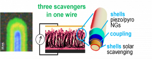
Kinetic, thermal and solar energies are ubiquitous at our surroundings under diverse forms, but their relatively low intensity and intermittent availability limit their potential recovery by microscale devices. These restrictions call for multi-source energy harvesters working under two principles: 1) combining different single-source harvesters in one device, or 2) using multifunctional materials capable of simultaneously converting various energy sources into electricity. In 1), efficiency per unit volume can decrease compared to the individual counterparts; in 2), materials as semiconductors, polymeric and oxide ferroelectrics and hybrid perovskites may act as multisource harvesters but huge advances are required to optimize their functionalities and sustainable fabrication at large scale.
I propose to fill the gap between these approaches offering an all-in-one solution to multisource energy scavenging, based on the nanoscale design of multifunctional three-dimensional materials. The demonstration of an industrially scalable one-reactor plasma/vacuum method will be crucial to integrate hybrid-scavenging components and to provide 3DScavengers materials with tailored microstructure-enhanced performance.
My ultimate goal is to build nanoarchitectures for simultaneous and enhanced individual scavenging applying photovoltaic, piezo- and pyro-electric effects, minimizing the environmental cost of their synthesis.
 |
Super-IcePhobic surfaces to prevent ice formation on aircraft (PHOBIC2ICE)
H2020-TRANSPORT/0149 PI: Agustín R. González-Elipe (Feb-2016/Jan-2019) |
Read more …
The accretion of ice represents a severe problem for aircraft, as the presence of even a scarcely visible layer can severely limit the function of wings, propellers, windshields, antennas, vents, intakes and cowlings. PHOBIC2ICE Project aims at developing technologies and predictive simulation tools for avoiding or mitigating this phenomenon.
PHOBIC2ICE project, by applying an innovative approach to simulation and modelling, will enable the design and fabrication of icephobic surfaces with improved functionalities. Several types of polymeric, metallic and hybrid coatings using different deposition methods will be developed. Laser treated and anodized surfaces will be prepared. Consequently, the Project focuses on collecting fundamental knowledge of phenomena associated with icephobicity issues. This knowledge will give better understanding of the ice accretion process on different coatings and modified surfaces. Certified research infrastructure (ice wind tunnel) and flight tests planned will aid in developing comprehensive solutions to address ice formation issue and will raise the Project’s innovation level.
The proposed solution will be environment-friendly, will contribute to the reduction of energy consumption, and will help eliminate the need for frequent on-ground de-icing procedures. This in turn will contribute to the reduction of cost, pollution and flight delay.
| Financial source: European Union
Code: H2020-TRANSPORT/0149 Acronym: PHOBIC2ICE |
Research team: Ana Borrás, Victor Rico. |
A full plasma and vacuum integrated process for the synthesis of high efficiency planar and 1D conformal perovskite solar cells (PlasmaPerovSol)H2020-MSCA-IF-2014 (Project ID: 661480) PI: Juan Ramón Sánchez Valencia (Jan-2016/Dec-2017) |
Read more …
Photovoltaic or solar cells (SC) devices –that transform light into electricity- have been extensively studied in the last decades since they represent a promising way to exploit the sun energy. Currently, perovskite-based solar cells(SC) are receiving increasing attention due to their low cost and high efficiency. They are very promising as an alternative for the existing ones, but still need to advance to reach higher efficiency and durability and require synthesis methods compatible with the industrial production of CMOS devices at wafer scale. These recent SC are mostly fabricated via wet methods in planar architecture. Inherent to the nature of the wet approaches, usually appear several drawbacks as contaminations and chemical reactions on the interfaces that might result deterioration of the SC performance.
PlasmaPerovSol main objective is the fabrication of a complete perovskite solar cell device by a full plasma and vacuum integrated process carried out under the premises of the “one reactor concept”. Thus, the different components of the solar cell will be deposited sequentially within a vacuum reactor avoiding exposition of the materials and interfaces to air or solvents. The technology developed by the hosting group combine vacuum deposition assisted by plasma that permits the fabrication of conformal layers over a large variety of templates. This approach is also proposed here to fabricate conformal multilayers over 1D scaffold that will push the advantages of one-dimensional SC. Plasma and vacuum processes present as advantage the high purity and stoichiometric control on the deposition within an ample range of materials compositions. The synthesis approach is compatible with large scale industrial production and allows the fabrication of SC on processable and flexible substrates. At the same time, the low temperatures used make the approach compatible with current CMOS technology and by using masks permits their integration on preformed devices.
|
Financial source: Acronym: PlasmaPerovSol Project ID: 661480 |
Research Supervisor: Research group: University Pablo de Olavide: Juan Antonio Anta, Jesús Idígoras |
FURTHER INFORMATION
|
NanoDevices3D (NanoD3D): Nanowires and Nanotrees for a new generation of self-powered nanodevices PI: Ana I Borrás (Nov-2017/Dec-2019) |
Read more …
|
Financial source: Ministerio de Economía y Competitividad. Acciones de Dinamización «Europa Investigación 2017» Code: EUIN2017-89059 Acronym: NanoD3D |
Research team: Juan R. Ramón Sánchez-Valencia, M.C. López-Santos. |
|
PIs: Francisco Yubero, Angel Barranco (Jan-2017/Dec-2019) |
Read more …
NANOFlow is a multidisciplinary Project that aims the development of novel optofluidics sensing devices integrating advanced multifunctional nanostructured materials. The project is solidly grounded in the research group experience in the synthesis of nanoestructured functional thin films, advance surface treatments and development of planar photonic structures The main objective of the project is to combine and integrate the available synthetic and processing methodologies in the fabrication of optofluidic components capable of modifying their physical behavior when they are exposed to liquids. The integration of these optofluidic components together with accessory technologies based on new principles of photonic detection, large surface area microplasmas discharge as light sources or flexible substrates for the fabrication of sensing tags define an ambitious landscape of applications that will be explored in the project. Besides, the modeling of thin film growth in combination with advanced deposition diagnosis methodologies will be combined to adjust the thin film deposition processes to the desired functionalities.Therefore, NANOFlow aims to cover all the scientific-technological chain from the materials development to the final applications including advanced characterization, flexible synthetic routes, alternative low-cost and high throughput process (e.g. atmospheric plasma synthesis), device integration and testing of devices in real conditions.
The NANOFlow research activities will culminate in the development of three innovative devices, namely smart labels for sensing, traceability and anticounterfeiting applications (e.g. smart labels incorporated in food-packaging), a versatile optofluidic multisensing device and an optofluidic photocatalytic cleaning system that will integrate a large area microplasma source, liquid actuated UV/Visible optical switches and a photocatalytic nanostructured surface. All of these devices will operate under the basis of an optofluidic actuation and/or response and are designed to present clear potentialities for direct application in liquid sensing, manipulation and monitoring.
The NANOFlow research activities in the different work-packages and, particularly, the final devices are intended to have a direct impact in the Theme 2 (Seguridad and Calidad Alimentaria) of the “RETOS” defined in the call covering this project proposal.. Besides, some of the activities proposed, in particular the third device are also connected with the Theme 3 (Energía segura eficiente y limpia) of the call. It is very interesting to stress that these activities are of particular relevance in the geographical context of Andalucia where Agriculture, Food production and Energy are three of the most relevant strategic sectors.
|
Financial source: Agencia Estatal de Investigación (AEI) y Fondo Europeo de Desarrollo Regional (FEDER) Code: MAT2016-79866-R Acronym: NANOFLOW
|
Research team: Agustin R. Gonzalez-Elipe (ICMS-CSIC), José Cotrino (ICMS-US), Juan Pedro Espinós (ICMS-CSIC), Fabián Frutos (US), Ana I. Borrás (ICMS-CSIC), Alberto Palmero (ICMS-CSIC), Victor Rico (ICMS-CSIC), Angel Barranco (ICMS-CSIC), F. Yubero (ICMS-CSIC), Ricardo Molina (IQAC-CSIC), Fernando Lahoz (ULL), Xerman de la Fuente (ICMA-CSIC), Jesús Cuevas (US), Mª Fe Laguna (UPM), Antonio Rodero (UCO), Mª Carmen García (UCO) Work team doctors: Juan R. Sánchez-Valencia, Francisco J. Aparicio, Jorge Gil-Rostra, Victor López, Rafael Alvarez, M.C. López-Santos, Francisco J. García, Ana M. Gómez, María Alcaire |
Monitorización en tiempo real de múltiples propiedades de fluidos mediante transductores fotónicos y electromagnéticos (REMO)Participant centers: Universidad Carlos III, Indra Sistemas S.A., Universidad Politécnica de Madrid, Repsol S.A PI (NToSP): Agustín R. González-Elipe (Sept-2015/Sept-2018) |
Apoyo tecnológicoFinancial source: Asociación de la Industria Navarra (AIN) PI: Agustín R González-Elipe (2015/2016) |